Solar cells made with quantum dots have achieved a new record efficiency, and been made more stable at the same time
One of the most promising, emerging solar cell technologies has received a major efficiency boost. Engineers at UNIST in South Korea have created quantum dot solar cells with a world record efficiency of 18.1%.
Quantum dots are essentially just tiny, circular semiconductor crystals that are incredibly efficient at absorbing and emitting light. The color of light they interact with can be set by changing their size, which makes them useful in display technologies or as sensors.
But where they might end up being most useful is in solar cells. Most commercial solar cells are made with bulk materials as the light-collecting layer, which means the whole surface absorbs the same wavelengths. But with quantum dots you can have multiple sizes that focus on a different part of the spectrum, boosting potential efficiency. As an added bonus, they’re cheap and easy to manufacture, and can even be made into a sprayable solution.
For the new study, researchers at UNIST tweaked the recipe a bit to improve the technology. Quantum dot solar cells made with organic materials have the highest theoretical efficiency, but unfortunately they suffer from defects that make them less stable in sunlight and weather – not ideal for devices designed to be out in the sun all day. To get around that, these solar cells are usually made with inorganic materials instead, but this limits their efficiency, the team says.
The UNIST team made their quantum dots out of an organic perovskite, and developed a new method for anchoring them to a substrate that allowed the dots to be placed closer together. This boosted the efficiency to a record-setting high of 18.1%, up from 16.6% in 2020. This record has been independently recognized by the National Renewable Energy Laboratory (NREL), which keeps an ongoing chart comparing the efficiency of different technologies.
Even better, the new solar cells were far more stable. They maintained their efficiency for 1,200 hours under normal conditions, and 300 hours at an elevated temperature of 80 °C (176 °F). They performed just as well after two years in storage.
Quantum dot solar cells still have a long way to go to catch up to the everyday silicon solar cells, the latter has had a half-century head-start and is rapidly approaching its theoretical maximum efficiency. Meanwhile, quantum dots have only really been in the lab since about 2010, when they had an efficiency of under 4%. Along with the efficiency gains, the inexpensive and simple manufacturing should help scale up the tech and make a wider range of surfaces photovoltaic.
Researchers at the Georgia Institute of Technology have created the world’s first functional semiconductor made from graphene, a single sheet of carbon atoms held together by the strongest bonds known. Semiconductors, which are materials that conduct electricity under specific conditions, are foundational components of electronic devices. The team’s breakthrough throws open the door to a new way of doing electronics.
Their discovery comes at a time when silicon, the material from which nearly all modern electronics are made, is reaching its limit in the face of increasingly faster computing and smaller electronic devices.
Walter de Heer, Regents’ Professor of physics at Georgia Tech, led a team of researchers based in Atlanta, Georgia, and Tianjin, China, to produce a graphene semiconductor that is compatible with conventional microelectronics processing methods—a necessity for any viable alternative to silicon.
In this latest research, published in Nature, de Heer and his team overcame the paramount hurdle that has been plaguing graphene research for decades, and the reason why many thought graphene electronics would never work. Known as the “band gap,” it is a crucial electronic property that allows semiconductors to switch on and off. Graphene didn’t have a band gap—until now.
“We now have an extremely robust graphene semiconductor with 10 times the mobility of silicon, and which also has unique properties not available in silicon,” de Heer said. “But the story of our work for the past 10 years has been, ‘Can we get this material to be good enough to work?'”
A new type of semiconductor
De Heer started to explore carbon-based materials as potential semiconductors early in his career, and then made the switch to exploring two-dimensional graphene in 2001. He knew then that graphene had potential for electronics.
“We were motivated by the hope of introducing three special properties of graphene into electronics,” he said. “It’s an extremely robust material, one that can handle very large currents, and can do so without heating up and falling apart.”
De Heer achieved a breakthrough when he and his team figured out how to grow graphene on silicon carbide wafers using special furnaces. They produced epitaxial graphene, which is a single layer that grows on a crystal face of the silicon carbide. The team found that when it was made properly, the epitaxial graphene chemically bonded to the silicon carbide and started to show semiconducting properties.
Over the next decade, they persisted in perfecting the material at Georgia Tech and later in collaboration with colleagues at the Tianjin International Center for Nanoparticles and Nanosystems at Tianjin University in China. De Heer founded the center in 2014 with Lei Ma, the center’s director and a co-author of the paper.
How they did it
In its natural form, graphene is neither a semiconductor nor a metal, but a semimetal. A band gap is a material that can be turned on and off when an electric field is applied to it, which is how all transistors and silicon electronics work. The major question in graphene electronics research was how to switch it on and off so it can work like silicon.
But to make a functional transistor, a semiconducting material must be greatly manipulated, which can damage its properties. To prove that their platform could function as a viable semiconductor, the team needed to measure its electronic properties without damaging it.
They put atoms on the graphene that “donate” electrons to the system—a technique called doping, used to see whether the material was a good conductor. It worked without damaging the material or its properties.
The team’s measurements showed that their graphene semiconductor has 10 times greater mobility than silicon. In other words, the electrons move with very low resistance, which, in electronics, translates to faster computing. “It’s like driving on a gravel road versus driving on a freeway,” de Heer said. “It’s more efficient, it doesn’t heat up as much, and it allows for higher speeds so that the electrons can move faster.”
The team’s product is currently the only two-dimensional semiconductor that has all the necessary properties to be used in nanoelectronics, and its electrical properties are far superior to any other 2D semiconductors currently in development.
“A long-standing problem in graphene electronics is that graphene didn’t have the right band gap and couldn’t switch on and off at the correct ratio,” said Ma. “Over the years, many have tried to address this with a variety of methods. Our technology achieves the band gap, and is a crucial step in realizing graphene-based electronics.”
Moving forward
Epitaxial graphene could cause a paradigm shift in the field of electronics and allow for completely new technologies that take advantage of its unique properties. The material allows the quantum mechanical wave properties of electrons to be utilized, which is a requirement for quantum computing.
“Our motivation for doing graphene electronics has been there for a long time, and the rest was just making it happen,” de Heer said. “We had to learn how to treat the material, how to make it better and better, and finally how to measure the properties. That took a very, very long time.”
According to de Heer, it is not unusual to see yet another generation of electronics on its way. Before silicon, there were vacuum tubes, and before that, there were wires and telegraphs. Silicon is one of many steps in the history of electronics, and the next step could be graphene.
“To me, this is like a Wright brothers moment,” de Heer said. “They built a plane that could fly 300 feet through the air. But the skeptics asked why the world would need flight when it already had fast trains and boats. But they persisted, and it was the beginning of a technology that can take people across oceans.”
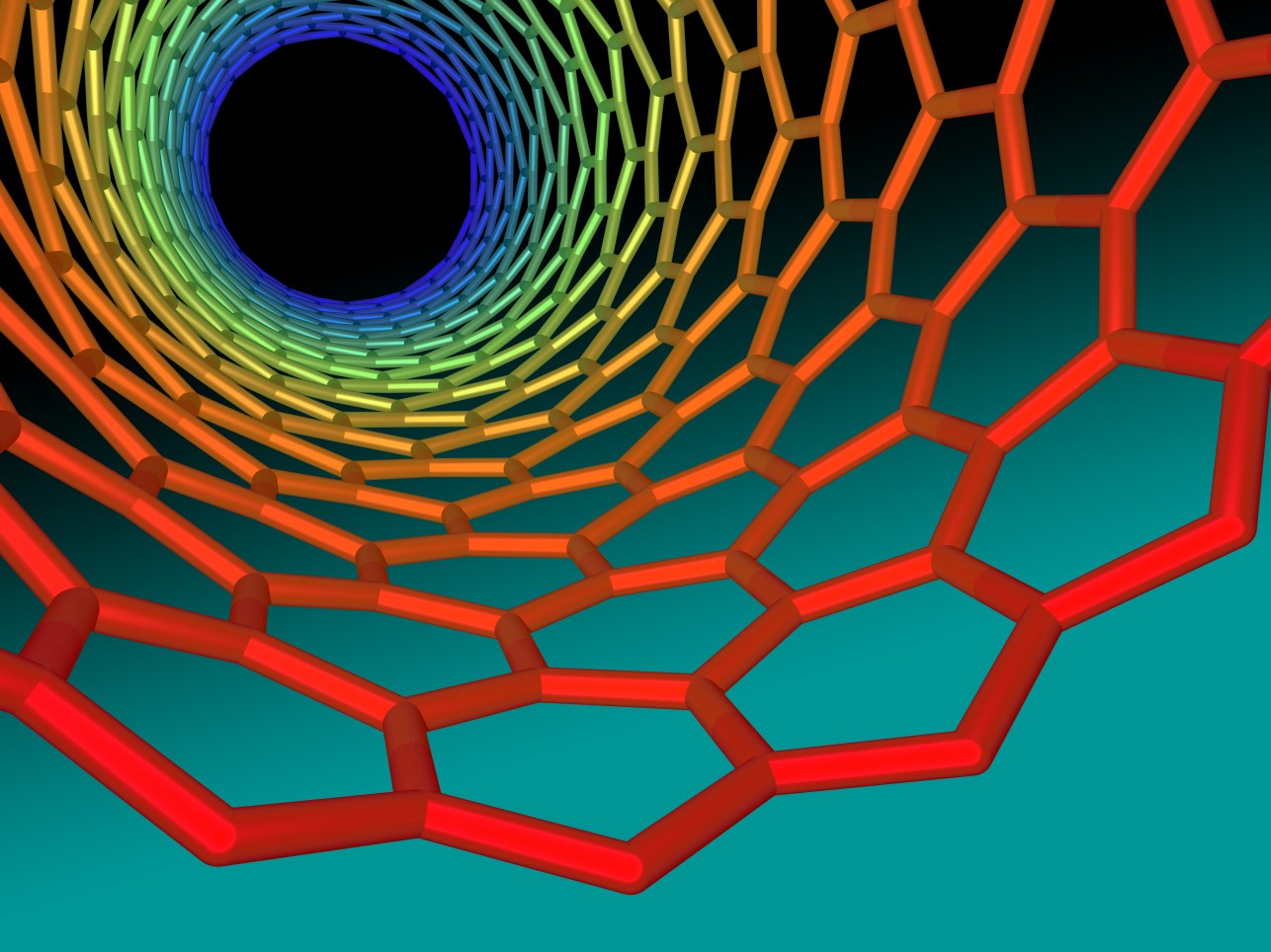
In an attempt to bring the next generation of computers to life, teams around the globe have been working with carbon nanotubes – one of the most conductive materials ever discovered. Now, for the first time ever, scientists made a transistor using carbon nanotubes that beats silicon.
For the first time, scientists have built a transistor out of carbon nanotubes that can run almost twice as fast as its silicon counterparts.
This is big, because for decades, scientists have been trying to figure out how to build the next generation of computers using carbon nanotube components, because their unique properties could form the basis of faster devices that consume way less power.
“Making carbon nanotube transistors that are better than silicon transistors is a big milestone,” said one of the team, Michael Arnold, from the University of Wisconsin-Madison. “This achievement has been a dream of nanotechnology for the last 20 years.”
First developed back in 1991, carbon nanotubes are basically minuscule carbon straws that measure just 1 atom thick.
Imagine a tiny, cylindrical tube that’s approximately 50,000 times smaller than the width of a human hair, and made from carbon atoms arranged in hexagonal arrays. That’s what a carbon nanotube wire would look like if you could see it at an atomic level.
Because of their size, carbon nanotubes can be packed by the millions onto wafers that can act just like a silicon transistor – the electrical switches that together form a computer’s central processing unit (CPU).
Despite being incredibly tiny, carbon nanotubes have some unique properties that make them an engineer’s dream.
“To put this into perspective,” says Washington-based carbon nanotubes producer, NanoScience Instruments, “if your hair had the same aspect ratio, a single strand would be over 40 metres long.”
And here’s the best part: just like that other 1-atom-thick wonder-material,graphene, carbon nanotubes are one of the most conductive materials ever discovered.
With ultra-strong bonds holding the carbon atoms together in a hexagonal pattern, carbon nanotubes are able to produce a phenomenon known aselectron delocalisation, which allows an electrical charge to move freely through it.
The arrangement of the carbon atoms also allows heat to move steadily through the tube, which gives it around 15 times the thermal conductivity and 1,000 times the current capacity of copper, while maintaining a density that’s just half that of aluminium.
Because of all these amazing properties, these semiconducting powerhouses could be our answer to the rapidly declining potential of silicon-based computers.
Right now, all of our computers are running on silicon processors and memory chips, but we’ve about hit the limit for how fast these can go. If scientists can figure out how to replace silicon-based parts with carbon nanotube parts, in theory, we could bump speeds up by five times instantly.
But there’s a major problem with mass-producing carbon nanotubes – they’re incredibly difficult to isolate from all the small metallic impurities that creep in during the manufacturing process, and these bits and pieces can interrupt their semiconducting properties.
But Arnold and his team have finally figured out how to get rid of almost all of these impurities. “We’ve identified specific conditions in which you can get rid of nearly all metallic nanotubes, where we have less than 0.01 percent metallic nanotubes,” he says.
As Daniel Oberhaus explains for Motherboard, the technique works by controlling the self-assembling properties of carbon nanotubes in a polymer solution, which not only allows the researchers to clean out impurities, but also to manipulate the proper spacing of nanotubes on a wafer.
“The end result are nanotubes with less than 0.01 percent metallic impurities, integrated on a transistor that was able to achieve a current that was 1.9 times higher than the most state-of-the-art silicon transistors in use today,” he says.
Simulations have suggested that in their purest form, carbon nanotube transistors should be able to able to perform five times faster or use five times less energy than silicon transistors, because their ultra-small dimensions allow them to very quickly switch a current signal as it travels across it.
This means longer-lasting phone batteries, or much faster wireless communications or processing speeds, but scientists have to actually build a working computer filled with carbon nanotube transistors before we can know for sure.
Arnold’s team has already managed to scale their wafers up to 2.5 by 2.5 cm transistors (1 inch by 1 inch), so they’re now figuring out how to make the process efficient enough for commercial production.
For the first time, scientists have built a transistor out of carbon nanotubes that can run almost twice as fast as its silicon counterparts.
This is big, because for decades, scientists have been trying to figure out how to build the next generation of computers using carbon nanotube components, because their unique properties could form the basis of faster devices that consume way less power.
“Making carbon nanotube transistors that are better than silicon transistors is a big milestone,” said one of the team, Michael Arnold, from the University of Wisconsin-Madison. “This achievement has been a dream of nanotechnology for the last 20 years.”
First developed back in 1991, carbon nanotubes are basically minuscule carbon straws that measure just 1 atom thick.
Imagine a tiny, cylindrical tube that’s approximately 50,000 times smaller than the width of a human hair, and made from carbon atoms arranged in hexagonal arrays. That’s what a carbon nanotube wire would look like if you could see it at an atomic level.
Because of their size, carbon nanotubes can be packed by the millions onto wafers that can act just like a silicon transistor – the electrical switches that together form a computer’s central processing unit (CPU).
Despite being incredibly tiny, carbon nanotubes have some unique properties that make them an engineer’s dream.
“To put this into perspective,” says Washington-based carbon nanotubes producer, NanoScience Instruments, “if your hair had the same aspect ratio, a single strand would be over 40 metres long.”
And here’s the best part: just like that other 1-atom-thick wonder-material, graphene, carbon nanotubes are one of the most conductive materials ever discovered.
With ultra-strong bonds holding the carbon atoms together in a hexagonal pattern, carbon nanotubes are able to produce a phenomenon known as electron delocalisation, which allows an electrical charge to move freely through it.
The arrangement of the carbon atoms also allows heat to move steadily through the tube, which gives it around 15 times the thermal conductivity and 1,000 times the current capacity of copper, while maintaining a density that’s just half that of aluminium.
Because of all these amazing properties, these semiconducting powerhouses could be our answer to the rapidly declining potential of silicon-based computers.
Right now, all of our computers are running on silicon processors and memory chips, but we’ve about hit the limit for how fast these can go. If scientists can figure out how to replace silicon-based parts with carbon nanotube parts, in theory, we could bump speeds up by five times instantly.
But there’s a major problem with mass-producing carbon nanotubes – they’re incredibly difficult to isolate from all the small metallic impurities that creep in during the manufacturing process, and these bits and pieces can interrupt their semiconducting properties.
But Arnold and his team have finally figured out how to get rid of almost all of these impurities. “We’ve identified specific conditions in which you can get rid of nearly all metallic nanotubes, where we have less than 0.01 percent metallic nanotubes,” he says.
As Daniel Oberhaus explains for Motherboard, the technique works by controlling the self-assembling properties of carbon nanotubes in a polymer solution, which not only allows the researchers to clean out impurities, but also to manipulate the proper spacing of nanotubes on a wafer.
“The end result are nanotubes with less than 0.01 percent metallic impurities, integrated on a transistor that was able to achieve a current that was 1.9 times higher than the most state-of-the-art silicon transistors in use today,” he says.
Simulations have suggested that in their purest form, carbon nanotube transistors should be able to able to perform five times faster or use five times less energy than silicon transistors, because their ultra-small dimensions allow them to very quickly switch a current signal as it travels across it.
This means longer-lasting phone batteries, or much faster wireless communications or processing speeds, but scientists have to actually build a working computer filled with carbon nanotube transistors before we can know for sure.
Arnold’s team has already managed to scale their wafers up to 2.5 by 2.5 cm transistors (1 inch by 1 inch), so they’re now figuring out how to make the process efficient enough for commercial production.
A team of researchers from across the country, led by Alexander Spott, University of California, Santa Barbara, USA, have built the first quantum cascade laser on silicon. The advance may have applications that span from chemical bond spectroscopy and gas sensing, to astronomy and free-space communications.
Integrating lasers directly on silicon chips is challenging, but it is much more efficient and compact than coupling external laser light to the chips. The indirect bandgap of silicon makes it difficult to build a laser out of silicon, but diode lasers can be built with III-V materials such as InP or GaAs. By directly bonding an III-V layer on top of the silicon wafer and then using the III-V layers to generate gain for the laser, this same group has integrated a multiple quantum well laser on silicon that operates at 2 µm. Limitations in diode lasers prevent going to longer wavelengths where there are many more applications, so the group turned their attention to using quantum cascade lasers instead.
Building a quantum cascade laser on silicon was a challenging task made more difficult by the fact that silicon dioxide becomes heavily absorptive at longer wavelengths in the mid-infrared.
“This meant that not only did we have to build a different type of laser on silicon, we had to build a different silicon waveguide too,” Spott explained. “We built a type of waveguide called a SONOI waveguide [silicon-on-nitride-on-insulator], which uses a layer of silicon nitride [SiN] underneath the silicon waveguide, rather than just SiO2.”
The breakthrough could lead to several applications, Spott explained. Traditionally, silicon photonic devices operate at near-infrared wavelengths, with applications in data transmission and telecommunications. However, there is emerging research interest in building these silicon photonic devices for longer mid-infrared wavelengths, for a range of sensing and detection applications, such as chemical bond spectroscopy, gas sensing, astronomy, oceanographic sensing, thermal imaging, explosive detection, and free-space communications.
The next step for the team is to improve the heat dissipation to improve the performance of these QCLs and to allow them to make continuous-wave QCLs on silicon. “We generally hope to improve the design to get higher powers and efficiency,” Spott said. “This brings us closer to building fully integrated mid-infrared devices on a silicon chip, such as spectrometers or gas sensors. Silicon is inexpensive, the fabrication can be scaled up to significantly reduce the cost of individual chips, and many small devices can be built on the same silicon chip for example multiple different types of sensors operating at different mid-infrared wavelengths.”
False-colour electron microscope image of the silicon nanoelectronic device which contains the phosphorus atom used for the demonstration of quantum entanglement.
A team of Australian engineers has proven—with the highest score ever obtained—that a quantum version of computer code can be written, and manipulated, using two quantum bits in a silicon microchip. The advance removes lingering doubts that such operations can be made reliably enough to allow powerful quantum computers to become a reality.
The result, obtained by a team at Australia’s University of New South Wales (UNSW) in Sydney, appears today in the international journal, Nature Nanotechnology.
The quantum code written at UNSW is built upon a class of phenomena called quantum entanglement, which allows for seemingly counterintuitive phenomena such as the measurement of one particle instantly affecting another – even if they are at opposite ends of the universe.
“This effect is famous for puzzling some of the deepest thinkers in the field, including Albert Einstein, who called it ‘spooky action at a distance’,” said Professor Andrea Morello, of the School of Electrical Engineering & Telecommunications at UNSW and Program Manager in the Centre for Quantum Computation & Communication Technology, who led the research. “Einstein was sceptical about entanglement, because it appears to contradict the principles of ‘locality’, which means that objects cannot be instantly influenced from a distance.”
Physicists have since struggled to establish a clear boundary between our everyday world—which is governed by classical physics—and this strangeness of the quantum world. For the past 50 years, the best guide to that boundary has been a theorem called Bell’s Inequality, which states that no local description of the world can reproduce all of the predictions of quantum mechanics.
Bell’s Inequality demands a very stringent test to verify if two particles are actually entangled, known as the ‘Bell test’, named for the British physicist who devised the theorem in 1964.
“The key aspect of the Bell test is that it is extremely unforgiving: any imperfection in the preparation, manipulation and read-out protocol will cause the particles to fail the test,” said Dr Juan Pablo Dehollain, a UNSW Research Associate who with Dr Stephanie Simmons was a lead author of the Nature Nanotechnology paper.
“Nevertheless, we have succeeded in passing the test, and we have done so with the highest ‘score’ ever recorded in an experiment,” he added.
Project leader Andrea Morello (left) with lead authors Stephanie Simmons (middle) and Juan Pablo Dehollain (right) in the UNSW laboratory where the experiments were performed.
In the UNSW experiment, the two quantum particles involved are an electron and the nucleus of a single phosphorus atom, placed inside a silicon microchip. These particles are, literally, on top of each other—the electron orbits around the nucleus. Therefore, there is no complication arising from the spookiness of action at a distance.
However, the significance of the UNSW experiment is that creating these two-particle entangled states is tantamount to writing a type of computer code that does not exist in everyday computers. It therefore demonstrates the ability to write a purely quantum version of computer code, using two quantum bits in a silicon microchip—a key plank in the quest super-powerful quantum computers of the future.
“Passing the Bell test with such a high score is the strongest possible proof that we have the operation of a quantum computer entirely under control,” said Morello. “In particular, we can access the purely-quantum type of code that requires the use of the delicate quantum entanglement between two particles.”
In a normal computer, using two bits one, could write four possible code words: 00, 01, 10 and 11. In a quantum computer, instead, one can also write and use ‘superpositions’ of the classical code words, such as (01 + 10), or (00 + 11). This requires the creation of quantum entanglement between two particles.
“These codes are perfectly legitimate in a quantum computer, but don’t exist in a classical one,” said UNSW Research Fellow Stephanie Simmons, the paper’s co-author. “This is, in some sense, the reason why quantum computers can be so much more powerful: with the same number of bits, they allow us to write a computer code that contains many more words, and we can use those extra words to run a different algorithm that reaches the result in a smaller number of steps.”
Morello highlighted the importance of achieving the breakthrough using a silicon chip: “What I find mesmerising about this experiment is that this seemingly innocuous ‘quantum computer code’ – (01 + 10) and (00 + 11) – has puzzled, confused and infuriated generations of physicists over the past 80 years.
“Now, we have shown beyond any doubt that we can write this code inside a device that resembles the silicon microchips you have on your laptop or your mobile phone. It’s a real triumph of electrical engineering,” he added.
Faster, smaller, greener computers, capable of processing information up to 1,000 times faster than currently available models, could be made possible by replacing silicon with materials that can switch back and forth between different electrical states.
The present size and speed limitations of computer processors and memory could be overcome by replacing silicon with ‘phase-change materials’ (PCMs), which are capable of reversibly switching between two structural phases with different electrical states – one crystalline and conducting and the other glassy and insulating – in billionths of a second.
Modelling and tests of PCM-based devices have shown that logic-processing operations can be performed in non-volatile memory cells using particular combinations of ultra-short voltage pulses, which is not possible with silicon-based devices.
In these new devices, logic operations and memory are co-located, rather than separated, as they are in silicon-based computers. These materials could eventually enable processing speeds between 500 and 1,000 times faster than the current average laptop computer, while using less energy. The results are published in the journal Proceedings of the National Academy of Sciences.
The processors, designed by researchers from the University of Cambridge, the Singapore A*STAR Data-Storage Institute and the Singapore University of Technology and Design, use a type of PCM based on a chalcogenide glass, which can be melted and recrystallized in as little as half a nanosecond (billionth of a second) using appropriate voltage pulses.
The calculations performed by most computers, mobile phones and tablets are carried out by silicon-based logic devices. The solid-state memory used to store the results of such calculations is also silicon-based. “However, as demand for faster computers continues to increase, we are rapidly reaching the limits of silicon’s capabilities,” said Professor Stephen Elliott of Cambridge’s Department of Chemistry, who led the research.
The primary method of increasing the power of computers has previously been to increase the number of logic devices which they contain by progressively reducing the size of the devices, but physical limitations for current device architectures mean that this is quickly becoming nearly impossible to continue.
Currently, the smallest logic and memory devices based on silicon are about 20 nanometres in size – approximately 4000 times thinner than a human hair – and are constructed in layers. As the devices are made ever smaller in order to increase their numbers on a chip, eventually the gaps between the layers will get so small that electrons which are stored in certain regions of flash non-volatile memory devices will be able to tunnel out of the device, resulting in data loss. PCM devices can overcome this size-scaling limit since they have been shown to function down to about two nanometres.
An alternative for increasing processing speed without increasing the number of logic devices is to increase the number of calculations which each device can perform, which is not possible using silicon, but the researchers have demonstrated that multiple calculations are possible for PCM logic/memory devices.
First developed in the 1960s, PCMs were originally used in optical-memory devices, such as re-writable DVDs. Now, they are starting to be used for electronic-memory applications and are beginning to replace silicon-based flash memory in some makes of smartphones.
The PCM devices recently demonstrated to perform in-memory logic do have shortcomings: currently, they do not perform calculations at the same speeds as silicon, and they exhibit a lack of stability in the starting amorphous phase.
However, the Cambridge and Singapore researchers found that, by performing the logic-operation process in reverse – starting from the crystalline phase and then melting the PCMs in the cells to perform the logic operations – the materials are both much more stable and capable of performing operations much faster.
The intrinsic switching, or crystallization, speed of existing PCMs is about ten nanoseconds, making them suitable for replacing flash memory. By increasing speeds even further, to less than one nanosecond (as demonstrated by the Cambridge and Singapore researchers in 2012), they could one day replace computer dynamic random-access memory (DRAM), which needs to be continually refreshed, by a non-volatile PCM replacement.
In a silicon-based system, information is shuffled around, costing both time and energy. “Ideally, we’d like information to be both generated and stored in the same place,” said Dr Desmond Loke of the Singapore University of Technology and Design, the paper’s lead author. “Silicon is transient: the information is generated, passes through and has to be stored somewhere else. But using PCM logic devices, the information stays in the place where it is generated.”
“Eventually, what we really want to do is to replace both DRAM and logic processors in computers by new PCM-based non-volatile devices,” said Professor Elliott. “But for that, we need switching speeds approaching one nanosecond. Currently, refreshing of DRAM leaks a huge amount of energy globally, which is costly, both financially and environmentally. Faster PCM switching times would greatly reduce this, resulting in computers which are not just faster, but also much ‘greener’.”
The research was part-funded by the UK Engineering and Physical Sciences Research Council (EPSRC).
Material scientists at Vanderbilt University have developed a supercapacitor made out of silicon. Previously thought to be kind of a crazy idea, the silicon capacitor can be built into a chip — which could give cellphones weeks of life from one charge, or solar cells that produce energy with or without the sun. Pretty sweet deal.Published in Scientific Reports, the first-ever silicon supercap stores energy by gathering ions on the surface of the porous material. Different from batteries, which work on chemical reactions, the silicon supercaps can be charged in minutes and last way longer. Silicon had been considered unsuitable for supercaps because of the way it reacts with the electrolytes that make the energy-storing ions.
“If you ask experts about making a supercapacitor out of silicon, they will tell you it is a crazy idea,” said assistant professor Cary Pint, who headed the development team at Vanderbilt. “But we’ve found an easy way to do it.”
Pint’s team coated the silicon in carbon — well, technically a few nanometers of graphene — and it stabilized the surface of the silicon, making it perfect for storing energy.
“All the things that define us in a modern environment require electricity,” said Pint. “The more that we can integrate power storage into existing materials and devices, the more compact and efficient they will become.”
Geekosystem is a Mashable publishing partner that aims to unite all the tribes of geekdom under one common banner. This article is reprinted with the publisher’s permission.


